Online Questions and Answers Topic Outline
- MCQs in FET Amplifiers
- MCQs in FET Small-Signal Model
- MCQs in JFET Fixed-Bias Configuration
- MCQs in JFET Self-Bias Configuration
- MCQs in JFET Voltage-Divider Configuration
- MCQs in JFET Source-Follower (Common-Drain) Configuration
- MCQs in JFET Common-Gate Configuration
- MCQs in Depletion-type MOSFETs
- MCQs in Enhancement-type MOSFETs
- MCQs in E-MOSFET Drain-Feedback Configuration
- MCQs in E-MOSFET Voltage-Divider Configuration
- MCQs in Designing FET Amplifier Networks
Practice Exam Test Questions
Choose the letter of the best answer in each questions.
1. FET amplifiers provide ________.- A) excellent voltage gain
- B) high input impedance
- C) low power consumption
- D) All of the above
- A) current
- B) voltage
- C) power
- D) resistance
- A) current
- B) voltage
- C) power
- D) resistance
- A) digital circuitry
- B) high-frequency
- C) buffering
- D) All of the above
- A) 1 µS to 10 µS
- B) 100 µS to 1000 µS
- C) 1000 µS to 5000 µS
- D) 10000 µS to 100000 µS
- A) 0 mA
- B) 0.25 IDSS
- C) 0.5 IDSS
- D) IDSS
- A) 100 kΩ
- B) 1 MΩ
- C) 10 MΩ
- D) 1000 MΩ
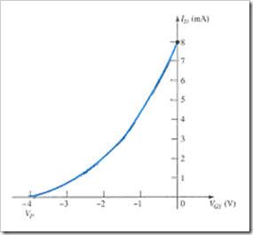
8. Referring to the transfer characteristics shown below, calculate gm at VGSQ = –1 V.
- A) 2 mS
- B) 3 mS
- C) 4 mS
- D) 5 mS
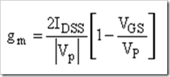
9. Use the following equation to calculate gm for a JFET having IDSS = 10 mA, VP = –5 V, and VGSQ = –2.5 V.
- A) 2 mS
- B) 3 mS
- C) 4 mS
- D) 5 mS
- A) 2 mS
- B) 2.5 mS
- C) 2.75 mS
- D) 3.25 mS
- A) 2.83 mS
- B) 3.00 mS
- C) 3.25 mS
- D) 3.46 mS
12. Referring to the figure below, determine the output impedance for VGS = –3 V at VDS = 5 V.
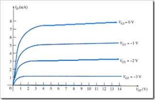
- A) 100 kΩ
- B) 80 kΩ
- C) 25 kΩ
- D) 5 kΩ
- A) 4 mS, 66.7 kΩ
- B) 4 mS, 15 kΩ
- C) 66.7 kΩ, 4 mS
- D) None of the above
14. The steeper the slope of the ID versus VGS curve, the ________ the level of gm.
- A) less
- B) same
- C) greater
- A) one-fourth
- B) one-half
- C) three-fourths
- D) two-thirds
- A) 1
- B) 0.707
- C) 0.5
- D) 1.414
17. The more horizontal the characteristic curves on the drain characteristics, the ________ the output impedance.
- A) less
- B) same
- C) greater
18. What is (are) the function(s) of the coupling capacitors C1 and C2 in an FET circuit?
- A) to create an open circuit for dc analysis
- B) to isolate the dc biasing arrangement from the applied signal and load
- C) to create a short-circuit equivalent for ac analysis
- D) All of the above
- A) from the dc biasing arrangement
- B) from the specification sheet
- C) from the characteristics
- D) All of the above
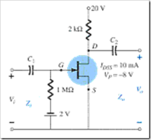
- A) 1.85 kΩ
- B) 1.92 kΩ
- C) 2.05 kΩ
- D) 2.15 kΩ
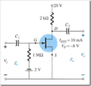
- A) –3.48
- B) –3.56
- C) –3.62
- D) –4.02
22. For the fixed-bias configuration, if rd < 10 • RD, then Zo = ________.
- A) RD
- B) RD || rd
- C) RG
- D) -gm • (RD || rd)
23. Which of the following is a required condition to simplify the equations for Zo and Av for the self-bias configuration?
- A) rd ≤ 10RD
- B) rd = RD
- C) rd ≥ 10RD
- D) None of the above
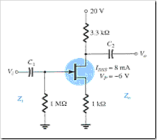
- A) 2.92 kΩ
- B) 3.20 kΩ
- C) 3.25 kΩ
- D) 3.75 kΩ
25. On which of the following parameters does rd have no or little impact in a source-follower configuration?
- A) Zi
- B) Zo
- C) Av
- D) All of the above
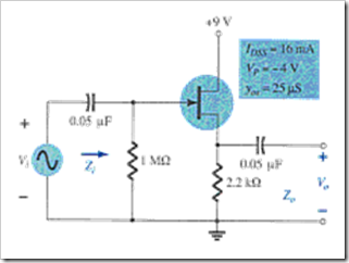
- A) 362.52 Ω
- B) 340.5 Ω
- C) 420.5 Ω
- D) 480.9 Ω
27. Referring to this figure, calculate Zi for yos = 20 µS. Assume VGSQ = −2.2V.
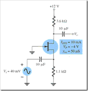
- A) 300.2 Ω
- B) 330.4 Ω
- C) 340.5 Ω
- D) 350.0 Ω
- A) VGSQ can be negative, zero, or positive.
- B) gm can be greater or smaller than gm0’.
- C) ID can be larger than IDSS’.
- D) All of the above
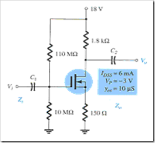
- A) –7.29
- B) –7.50
- C) –8.05
- D) –8.55
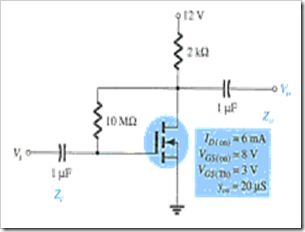
- A) 2.42 MΩ
- B) 2.50 MΩ
- C) 2.53 MΩ
- C) 2.59 MΩ
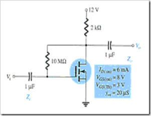
- A) 1.75 kΩ
- B) 1.81 kΩ
- C) 1.92 kΩ
- D) 2.00 kΩ
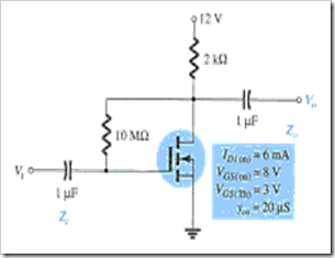
- A) –2.85
- B) –3.26
- C) –2.95
- D) –3.21
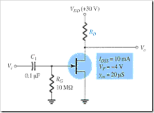
- A) 1.51 kΩ
- B) 1.65 kΩ
- C) 1.85 kΩ
- D) 2.08 kΩ
34. Referring to this figure, calculate the value of RD if the ac gain is 10. Assume VGSQ = ¼Vp.
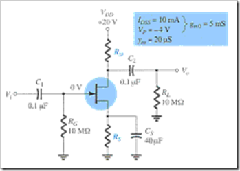
- A) 2.2 kΩ
- B) 2.42 kΩ
- C) 2.62 kΩ
- D) 2.82 kΩ
35. For an FET small-signal amplifier, one could go about troubleshooting a circuit by ________.
- A) viewing the circuit board for poor solder joints
- B) using a dc meter
- C) applying a test ac signal
- D) All of the above
Fill-in-the-blanks Questions
1. A field-effect transistor amplifier provides excellent voltage gain with the added feature of a _____ input impedance.
- A) low
- B) medium
- C) high
- D) None of the above
2. The depletion MOSFET circuit has a _____ input impedance than a similar JFET configuration.
- A) much higher
- B) much lower
- C) lower
- D) higher
3. The _____ is quite popular in digital circuits, especially in CMOS circuits that require very low power consumption.
- A) JFET
- B) BJT
- C) D-type MOSFET
- D) E-type MOSFET
- A) Zi
- B) gm
- C) ID
- D) IG
- A) Ai
- B) Av
- C) Zi
- D) Zo
- A) ID’, VGS
- B) VGS’, ID
- C) IG’, VDS
- D) IG’, ID
- A) ID to VGS
- B) ID to VDS
- C) VGS to IG
- D) VGS to VDS
- A) decreases
- B) remains the same
- C) increases
- D) None of the above
- A) Vp
- B) 0.5 Vp
- C) 0.3 Vp
- D) IDSS
10. The value of gm is at its maximum gm0 at VGS equal to _____ and zero at VGS equal to _____.
- A) 0 V, Vp
- B) Vp, 0 V
- C) 0.5Vp, 0.3Vp
- D) 0.3Vp , 0.5Vp
- A) 1 kΩ –10 kΩ
- B) 100 kΩ –1 MΩ
- C) 10 MΩ –100 MΩ
- D) 1012 Ω to 1015 Ω
- A) 5 µS –10 µS
- B) 10 µS –50 µS
- C) 50 µS –100 µS
- D) 200 µS –500 µS
13. The _____ configuration has the distinct disadvantage of requiring two dc voltage sources.
- A) self-bias
- B) voltage-divider
- C) fixed-bias
- D) All of the above
14. _____ is the network-input impedance for a JFET fixed-bias configuration.
- A) RG
- B) RD
- C) Zero
- D) None of the above
- A) Setting IG equal to zero
- B) Setting Vi equal to zero
- C) Setting ID equal to IDSS
- D) None of the above
- A) Fixed-bias
- B) Self-bias
- C) Voltage-divider
- D) All of the above
17. _____ is the only parameter that is different between voltage-divider and fixed-bias configurations.
- A) Zi
- B) Av
- C) Zo
- D) None of the above
18. The input and output signals are in phase in a _____ configuration.
- A) fixed-bias
- B) source-follower
- C) voltage-divider
- D) self-bias
- A) fixed-bias
- B) self-bias
- C) source-follower
- D) voltage-divider
20. The input and output signals are 180º out of phase in a _____ configuration.
- A) source-follower
- B) common-gate
- C) common-drain
- D) voltage-divider
21. The isolation between input and output circuits in the ac equivalent circuit is lost in a _____ configuration.
- A) common-gate
- B) common-source
- C) common-drain
- D) None of the above
22. The _____ configuration has an input impedance, which is other than RG.
- A) common-source
- B) common-gate
- C) common-drain
- D) None of the above
23. The gate-to-source voltage VGS of a(n) _____ must be larger than the threshold VGS(Th) for the transistor to conduct.
- A) JFET
- B) D-type MOSFET
- C) E-type MOSFET
- D) None of the above
24. rd changes from one operation region to another with _____ values typically occurring at _____ levels of VGS (closer to zero).
- A) lower, lower
- B) lower, higher
- C) higher, lower
- D) None of the above
- A) JFET
- B) D-type MOSFET
- C) E-type MOSFET
- D) None of the above
Check your work.
Complete List of Chapter Quiz in Electronic Devices and Circuit Theory
credit: Robert L. Boylestad© 2014 www.PinoyBIX.org


Post a Comment