This is the Multiple Choice Questions in Field-Effect Transistors (FETs) from the book Electronic Devices - Electron Flow Version and Conventional Current Version 8th Edition by Thomas L. Floyd. If you are looking for a reviewer in Electronics Engineering this will definitely help. I can assure you that this will be a great help in reviewing the book in preparation for your Board Exam. Make sure to familiarize each and every questions to increase the chance of passing the ECE Board Exam.
Online Questions and Answers Topic Outline
- MCQs in Field-Effect Transistors (FETs) | MCQs in JFET | MCQs in JFET Characteristics and Parameters | MCQs in JFET Biasing | MCQs in The Ohmic Region | MCQs in MOSFET | MCQs in MOSFET Characteristics and Parameters | MCQs in MOSFET Biasing | MCQs in IGBT
Practice Exam Test Questions
Choose the letter of the best answer in each questions.
1. On the drain characteristic curve of a JFET for VGS = 0, the pinch-off voltage is
- A) below the ohmic area.
- B) between the ohmic area and the constant current area.
- C) between the constant current area and the breakdown region.
- D) above the breakdown region.
2. For a JFET, the value of VDS at which ID becomes essentially constant is the
- A) pinch-off voltage.
- B) cutoff voltage.
- C) breakdown voltage.
- D) ohmic voltage.
- A) pinch-off voltage.
- B) cutoff voltage.
- C) breakdown voltage.
- D) ohmic voltage.
4. For a JFET, the change in drain current for a given change in gate-to-source voltage, with the drain-to-source voltage constant, is
- A) breakdown.
- B) reverse transconductance.
- C) forward transconductance.
- D) self-biasing.
- A) a metal oxide layer.
- B) a large input resistor to the device.
- C) an intrinsic layer.
- D) the gate-source junction being reverse-biased.
- A) a depletion MOSFET.
- B) an enhancement MOSFET.
- C) a VMOSFET.
- D) either a depletion or an enhancement MOSFET.
- A) diode
- B) JFET
- C) MOSFET
- D) bipolar junction transistor
8. A self-biased n-channel JFET has a VD = 6 V. VGS = –3 V. Find the value of VDS.
- A) –3 V
- B) –6 V
- C) 3 V
- D) 6 V

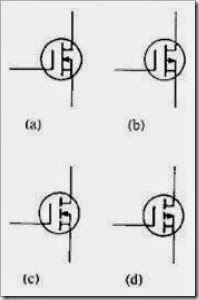
Figure 8-1
- A) a
- B) b
- C) c
- D) d
- A) a
- B) b
- C) c
- D) d
- A) a
- B) b
- C) c
- D) d
- A) a
- B) b
- C) c
- D) d

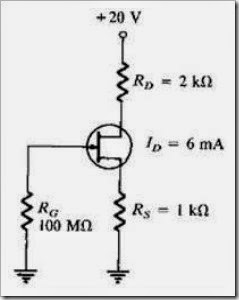
Figure 8-2
- A) –6 V
- B) 6 V
- C) 12 V
- D) –3 V
- A) 13.2 V
- B) 10 V
- C) 6.8 V
- D) 0 V
- A) –9 V
- B) 9 V
- C) 6 V
- D) –3 V
16. A JFET data sheet specifies VGS(off) = –6 V and IDSS = 8 mA. Find the value of ID when VGS = –3 V.
- A) 2 mA
- B) 4 mA
- C) 8 mA
- D) none of the above
17. A JFET data sheet specifies VGS(off) = –10 V and IDSS = 8 mA. Find the value of ID when VGS = –3 V.
- A) 2 mA
- B) 1.4 mA
- C) 4.8 mA
- D) 3.92 mA

Figure 8-3
- A) 20 V
- B) 8 V
- C) 6 V
- D) 2 V
- A) 20 V
- B) 8 V
- C) 6 V
- D) 2 V
- A) 6 mA
- B) 4 mA
- C) 2 mA
- D) 0 mA
- A) –20 V
- B) –8 V
- C) –6 V
- D) –2 V
- A) 0 V
- B) 2 V
- C) 4 V
- D) –2 V
23. The JFET is always operated with the gate-source pn junction _____ -biased.
- A) forward
- B) reverse
24. What three areas are the drain characteristics of a JFET (VGS = 0) divided into?
- A) ohmic, constant-current, breakdown
- B) pinch-off, constant-current, avalanche
- C) ohmic, constant-voltage, breakdown
25. What type(s) of gate-to-source voltage(s) can a depletion MOSFET (D-MOSFET) operate with?
- A) zero
- B) positive
- C) negative
- D) any of the above
- A) D-MOSFET
- B) E-MOSFET
- C) V-MOSFET
27. All MOSFETs are subject to damage from electrostatic discharge (ESD).
- A) true
- B) false
28. Midpoint bias for a D-MOSFET is ID = _____, obtained by setting VGS = 0.
- A) IDSS / 2
- B) IDSS / 3.4
- C) IDSS
- A) 0
- B) cannot be determined from information above
30. If VD is less than expected (normal) for a self-biased JFET circuit, then it could be caused by a(n)
- A) open RG.
- B) open gate lead.
- C) FET internally open at gate.
- D) all of the above
- A) VD.
- B) VGS.
- C) VS.
- D) VDS.
Check your work.
Complete List of Chapter MCQs in Floyd's Electronic Devices
credit: © 2014 www.PinoyBIX.org


Post a Comment